
VHDL Notes
Overview
Combinational logic, in which the output signals depend only on the current input signals
Sequential logic, in which the output depends both on current input and the past history of inputs. In other words, sequential logic is combinational logic with memory.
FPGA
The Virtex II FPGA:
A logic cell consists of a lookup table, a flip flop, and connection to adjacent cells.
The lookup table uses combinatorial logic to implement a 4-input expression (and, or, nand, addition, etc.)
A logic slice consists of 2 logic cells.
Xilinx counts closer to 2.25 logic cells per slice because they can do more per configurable logic block (CLB) than other architectures.
A CLB consists of 4 slices, but differs between different FPGAs.
This combined architecture gives benefits in the final system such as increased performance of logic execution.
It is important to note that the efficiency of a gate in an FPGA is not equivalent to that of a gate in an ASIC.
For example, a 1M gate FPGA is roughly equivalent to a 100K gate ASIC.
LUTs
Basically though, just a truth table (X inputs, X outputs) that can generate a function you want - think Karnaugh maps, binary rules etc.
Reset
Two types:
Synchronous
Asynchronous
What is used depends on your design.
Reset will be buffered from a reset buffer tree, it is wise to limit the amount of logic the reset must traverse once it reaches the local logic.
Synchronous
Usually recommended since your design can be a completely synchronous circuit
+Filters out the small glitches that can occur
-May need a pulse stretcher on the reset to make it edge triggered, consider multi-clock designs
-If the reset input isn't asserted on a clk edge, then the reset may be missed
If the design disables the clk to save power (eg. a processor), likewise the reset will be as well.
Asynchronous
Due to varying network skews this can lead to different FFs coming out of reset on different clock cycles giving an indeterminate behavior.
For a large reset network with a huge fan-out we can assume the network skew to be considerable - which further worsens the situation and increases the likelihood of problems.
-They are asynchronous, both at the assertion and at the de-assertion of the reset. The assertion is a non issue, the de-assertion is the issue. If the asynchronous reset is released at or near the active clock edge of a flip-flop, the output of the flip-flop could go metastable and thus the reset state of the ASIC could be lost.
-Asynchronous reset can have, depending on its source, is spurious resets due to noise or glitches on the board or system reset. A different but similar problem exists for synchronous resets if these spurious reset pulses occur near a clock edge, the flip-flops can still go metastable (but this is true of any data input that violates setup requirements).
Reset times
Recovery time: minimum time that an asynchronous control input pin must be stable before the next active clock edge transition. Like
T(su)Removal time: minimum time that an asynchronous control input pin must be stable before being deasserted and after the previous active clock transition. Like
T(h)
reset ________________
           | Recovery |______

clk                    _______
      ________________|
Removal Timing Check
A removal timing check ensures that there is adequate time between an active clock edge and the release of an asynchronous control signal. The check ensures that the active clock edge has no effect because the asynchronous control signal remains active until removal time after the active clock edge.
In other words, the asynchronous control signal is released (becomes inactive) well after the active clock edge so that the clock edge can have no effect
Recovery Timing Check
A recovery timing check ensures that there is a minimum amount of time between the asynchronous signal becoming inactive and the next active clock edge. In other words, this check ensures that after the asynchronous signal becomes inactive, there is adequate time to recover so that the next active clock edge can be effective.
For example, consider the time between an asynchronous reset becoming inactive and the clock active edge of a flip-flop. If the active clock edge occurs too soon after the release of reset, the state of the flip-flop may be unknown.
Delays
Setup time:
T(su)is the minimum amount of time a synchronous data input should be held STEADY BEFORE the clock'event so that the data input is reliably sampled by the clock event.Hold time:
T(h)is the minimum amount of time a synchronous data input should be held STEADY AFTER the clock event so that the data input is reliably sampled by the clock event.Hold time is usually zero or negative; if neg, that means the data input can change before the clk edge and still have a stable output.
Propagation delays:
T(p)is the delay for 0 -> 1 or 1 -> 0 for example, and these delays may not be symmetrical!
As usual, a diagram does wonders:

Metastability
When two inputs, such as data and clock or clock and reset, are changing at about the same time.
The solution is to reduce either
T(h)orT(su)but can't reduce both simultaneously.Can be achieved by chaining two flip-flops together so either the
T(su)orT(h)increases therefore reducing the probability of metastability
Minimum Clock period
So by summing up the T(su), T(h) and T(p); there will be a minimum clock period T(min) and therefore a maximum frequency F(max) for a particular circuit design.
Example:
T(su) = 0.6 ns
T(h)  = 0.4 ns
0.8 ns >= T(p) <= 1.0 ns

T(delay) of k-input gate = 1 + 0.1k ns

T(min) = 1/F(max) : critical path

-- Look at max frequency
T(min) = MAX{T(p)} + T(NOT GATE) + T(su)
       = 1.0       + 1.1         + 0.6
       = 2.7 ns
F(max) = 370 MHz

-- Check for hold time violations; if T(min) < T(h), then we can't achieve the
-- required T(h) for stable signals
T(min delay) = MIN{T(p)} + T(NOT GATE)
             = 0.8       + 1.1
             = 1.9 ns > T(h) = 0.4 ns
No violation!
Clock skew
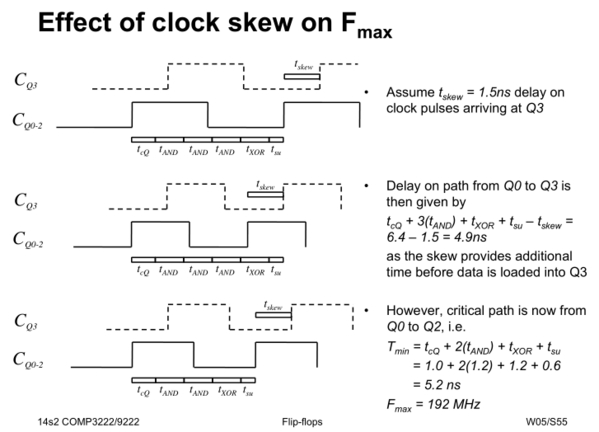
Positive clock skew means that the clock arriving a little slower in a counter-flip flop for example. This allows 'extra' time when calculating the critical path for a certain flip-flop.
A negative clock skew, i.e. clock arriving earlier at
Q3than atQ0–Q2would have the opposite effect of lengthening the clock period & reducing clock frequency
Latches
Okay, there are 2 huge differences here:
Normal (SR) latch
Gated latches
Both are asynchronous circuits
Normal latches
These are fucked, you don't want to ever write these!
It holds a bit value BUT its final state of the output depends on oscillatory behavior that depends on the speed of the gates and wires!
Gated latches
The have a
clkinput that has a conditionif = '1'then, output assignment. These aren't edge triggered!Like flip flops, they have implied memory.
SR latch has an illegal condition since in its truth table, it has has outputs (Q, Q') that aren't complements of one another!
S = set, R = reset; so yes, it is a 3 input LUT
D latch has no reset so it's like a D flip flip but while
clk=1, output state can change.
Below is the timing differences:

-- Example of implied memory, latch
-- equal is assigned at based on speed of gates + wires
-- so oscillatory behavior may have 'glitches'
process (A,B)
begin
    if A = B then
        equal <= '1';
    end if;
end process;
Gated SR latch
Can be made with OR gates or NAND gates; the latter uses less transistors and has the same characteristic table.
These are fucked since it has an undefined output when
S = R = 1- see last row since Q, q' aren't complements
0
x
x
no change
1
0
0
no change
1
0
1
0
1
1
0
1
1
1
1
x
Gated D Latch
Holds value and has no restricted combination
0
X
no change
1
0
0
1
1
1
-- Example of Gated D latch
-- NOTE that it's not edge triggered!
-- Sensitivity list is VERY important, if you miss the input D
-- synthesis tools will fuck up your latch
process (clk, D)
begin
    if clk = '1' then
        Q <= D;
    end if;
end process;
Flip flops
Like latches, its outputs change when
clk=1but are edge sensitive!Positive edge triggered D flip flops saves some gates and an inverter.
D Flip Flop
Synchronous circuits
You can also have an async reset
Values changes only on rising edges and holds value otherwise.
Rising edge
0
0
Rising edge
1
1
Non-Rising
X
Q
-- Example of D flip flop
process (clk)
begin
    if rising_edge(clk) then
        Q <= D;
    end if;
end process;
T Flip flop
Q changes when rising_edge(clk) and when T = 1
0
Q(t)
1
Q'(t)
Shift registers
Serial-in and serial-out (SISO)
Useful for buffering data serially
Essentially if you had a 4 bit reg. with 0000
Shift in D = 1, 0, 1, 1
After 4 clk cycles, reg. with 1011
Serial-in, parallel-out (SIPO)
You get the output of the reg. in 'real-time' and is useful converting serial input to parallel data.
Parallel-in, Parallel-out (PIPO)
if rising_edge(clk) then
    if L = '1' then
        Q <= R ;        -- load in data parallel
    else
        Q(0) <= Q(1) ;  -- shift data to right
        Q(1) <= Q(2) ;
        Q(2) <= Q(3) ;
        Q(3) <= w ;
    end if;
FSM
Moore
Output is purely a function of the present state. Not dependent upon inputs.
eg. counting number of D = 1 (input) on a clock edge, updated AFTER current clock cycle, doesn't care about current INPUT
Mealy
Output is also a function of its current inputs.
eg. counting number of D = 1 (input) on a clock edge, updated in 'real-time'
Tri State Buffers

Y <= A when (EN = '0') else 'Z';

-- for multiple buffers in parallel
tristate : for i in 0 to N generate
begin
    Y(i) <= A(i) when EN(i) = '1' else 'Z';
end generate tristate;
useful for replacing a MUX - eg. you have multiple data and selecting which to go on bus, you can disable ALL, and not just one.
Z = high impedance: influence on the rest of the circuit is removed, and the circuit node will be "floating" if no other circuit element determines its state
also keeps the same current into parallel (split into 4 eg)
Binary operations
Multiplication
// just like normal multiplication

    1101    // 13
    0101 x  // 5
    ----
    1101    // consider these as partial sums eg. p0
   0000-    // p1
  1101--    // p2
  ------
 1000001    // 65

 ----------------------------------------------------------

 // just do a partial sum

 // if a[0] = 0; 00000000 & b[7:0] = same as multiplying by 0
 p0[7:0] = a[0] × b[7:0] = {8{a[0]}} & b[7:0]
 p1[7:0] = a[1] × b[7:0] = {8{a[1]}} & b[7:0]
 p2[7:0] = a[2] × b[7:0] = {8{a[2]}} & b[7:0]
 p3[7:0] = a[3] × b[7:0] = {8{a[3]}} & b[7:0]
 p4[7:0] = a[4] × b[7:0] = {8{a[4]}} & b[7:0]
 p5[7:0] = a[5] × b[7:0] = {8{a[5]}} & b[7:0]
 p6[7:0] = a[6] × b[7:0] = {8{a[6]}} & b[7:0]
 p7[7:0] = a[7] × b[7:0] = {8{a[7]}} & b[7:0]

 // where {8{a[0]}} means repeating a[0] (the 0th bit of a) 8 times

 answer = p0 + (p1 << 1) + (p2 << 2) ...

  ----------------------------------------------------------

  // In HW

  100 // multiplicand
  011 // multiplier
  ---
  xxx // product
Division
Examples
4 bit counter

Last updated